The Silicon Photonics Connectivity Ecosystem and SENKO’s Role
Understanding the Silicon Photonics Ecosystem
Silicon photonics is revolutionizing data communication, high-performance computing, and next-generation networking by enabling faster, more efficient data transmission using light rather than electrical signals. This transformative technology relies on a composition of Chip Companies, OSATs (Outsourced Semiconductor Assembly and Test providers), and Foundries, each playing a crucial role in advancing CoPackaged Optics (CPO) and next-generation photonic integration. At the center of this ecosystem is SENKO’s MPC Connector, providing cutting-edge optical connectivity tailored to the specific needs of each sector. This article explores how SENKO addresses the unique challenges of Chip Design, OSAT manufacturing, and Foundry integration to drive the next era of high-speed networking.

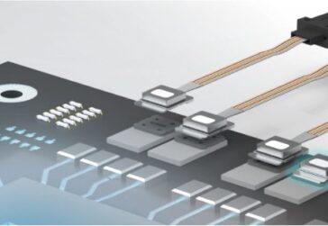
The Importance of SENKO’s Metallic PIC Connector (MPC)
In this rapidly evolving ecosystem, efficient optical connectivity solutions are essential to bridge silicon photonics chips with the broader network infrastructure. SENKO, a global leader in fiber optic connectivity solutions, plays a crucial role with the MPC connector. As silicon photonics drives ever-higher data rates, SENKO’s MPC connectors provide a high-density, multi-fiber interconnect solution that enables seamless optical fiber connection directly to the chip. These connectors are designed as a scalable solution that minimizes signal loss. SENKO’s MPC is designed to be compatible with the rigorous requirements of OSAT providers and semiconductor foundries, making the assembly and testing process more efficient.
Chip Companies
Silicon photonic chip companies design and develop photonic integrated circuits (PICs) that leverage silicon as the core material. These companies drive innovations in transceivers, modulators, and photodetectors to create high-speed, low-power optical solutions. Their role is critical in defining the architecture and performance benchmarks for silicon photonics applications in data centers, telecommunications, and artificial intelligence workloads.
SENKO supports the chip design optimization of these companies by ensuring high-performance optical interfaces that align with chip architectures. By enabling compact optical I/O placement, the shoreline density can be increased to maximize connectivity in tight silicon footprints. The mechanical packaging constraints can be addressed through connector miniaturization while supporting efficient heat dissipation for high-power optical applications.
Semiconductor Foundries
Semiconductor foundries manufacture silicon photonic chips based on designs provided by chip companies. These foundries have the advanced fabrication capabilities required for precise lithography, etching, and deposition processes to create photonic circuits at nanometer-scale dimensions. Key players in this space ensure that the silicon photonic devices meet stringent performance, reliability, and yield standards.
SENKO works closely with foundries to provide high-efficiency light coupling solutions to ensure precise fiber alignment through beam profiling for PICs. SENKO’s solution supports integration into foundry Process Design Kits (PDKs) for seamless adoption. In addition, early-stage optical validation can be achieved with wafer-level testing during fabrication.
Outsourced Semiconductor Assembly and Test (OSAT) Providers
Outsourced Semiconductor Assembly and Test (OSAT) providers are responsible for mass-producing and validating silicon photonics packages. They handle packaging, assembly, and final testing of silicon photonic devices. Packaging is a crucial step in ensuring that photonic chips are integrated with optical fibers and electronic circuits for real-world applications. OSAT providers specialize in high-precision alignment techniques, thermal management solutions, and testing procedures to guarantee functionality and performance consistency.
SENKO’s MPC is designed to support high volume manufacturing with precision alignment to achieve high-yield assembly and testing. Being able to withstand high-temperature assembly processes makes it compatible with reflow processes. Epoxy dispense optimization also enables efficient bonding techniques for photonic components.
Enabling the Future of Silicon Photonics
As data rates continue to surge, the role of a seamless silicon photonics connectivity ecosystem becomes even more crucial. With silicon photonics chips pushing the limits of performance, semiconductor foundries perfecting fabrication, and OSAT providers ensuring robust packaging, SENKO’s advanced connectivity solutions serve as a vital enabler of the entire value chain.
By providing cutting-edge MPC technology, SENKO is not only addressing today’s connectivity challenges but also paving the way for the next era of ultra-fast, energy-efficient, and scalable optical networking solutions. As the silicon photonics industry advances, SENKO will continue to play a key role in shaping the future of high-speed connectivity.

データセンター